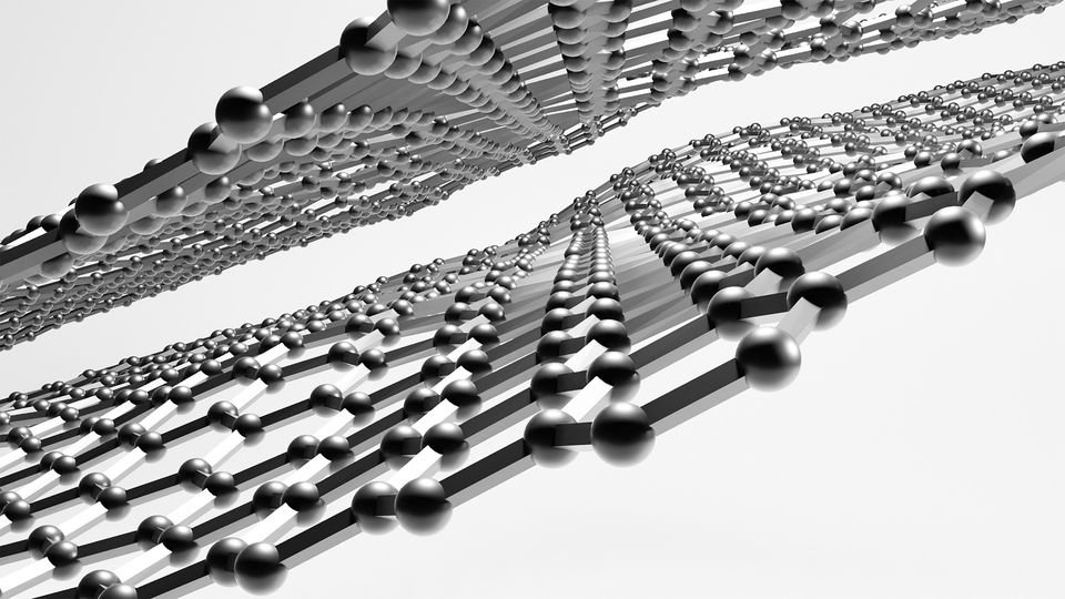
Graphene has transformed modern material science. However, its performance depends heavily on its structure, thickness, and quality. Even a small variation in the number of layers can change electrical, mechanical, and thermal behavior. Because of this, accurate characterization becomes essential before using it in any application.
Researchers focus on identifying layer count, structural defects, surface chemistry, and overall material quality. This is especially important when working with single-layer graphene, where even minor inconsistencies can affect performance. Therefore, scientists rely on a combination of advanced techniques to analyze graphene at both the microscopic and atomic levels.
So, how do researchers characterize graphene layers effectively? Let’s explore the most reliable methods with technical clarity.
Optical Microscopy for Initial Layer Identification
Researchers often begin with optical microscopy because it provides a fast and simple way to locate graphene flakes. When graphene is placed on substrates such as silicon dioxide (SiO₂), optical contrast appears due to light interference effects. Because of this:
- Single layers appear faint but are still distinguishable
- Few-layer graphene shows a darker contrast
- Thickness variations become visible across the surface
Although this method does not provide precise measurements, it serves as a quick screening step before detailed analysis.
Raman Spectroscopy for Layer Count and Defect Analysis
Raman spectroscopy remains the most important technique for graphene characterization. It analyzes how light interacts with vibrational modes of carbon atoms, which directly reflects the material’s electronic structure. Key Raman features include:
- G band (~1580 cm⁻¹): Represents in-plane vibrations of sp² carbon atoms
- 2D band (~2700 cm⁻¹): Indicates layer count and stacking behavior
- D band (~1350 cm⁻¹): Shows defects or disorder in the lattice
For single-layer graphene, the 2D peak appears sharp and symmetric, and the intensity ratio I₂D/I_G is typically greater than 2. As layers increase, this peak broadens, and the ratio decreases.
Because of this, Raman spectroscopy provides a reliable and non-destructive way to determine both quality and layer count.
Atomic Force Microscopy for Thickness Measurement
Atomic Force Microscopy (AFM) provides nanoscale height measurements using a sharp probe that scans the surface.
Researchers often use AFM to determine the thickness of graphene. However, there is an important distinction between theoretical and measured values.
- The theoretical thickness of a single graphene layer is ~0.34 nm
- The measured thickness on substrates is typically ~0.8–1.0 nm
This difference occurs due to surface contamination, trapped air layers, and substrate interactions. Because of this:
- AFM helps confirm layer presence and uniformity
- Surface roughness and defects become visible
- Wrinkles, folds, and residues can be identified
Understanding this “apparent thickness” prevents misinterpretation of layer count.
Transmission Electron Microscopy for Atomic Structure
Transmission Electron Microscopy (TEM) provides direct visualization of graphene’s atomic structure. By transmitting electrons through the material, it produces high-resolution images. Because of this:
- Atomic lattice patterns become visible
- Layer stacking can be analyzed precisely
- Grain boundaries and defects can be detected
In addition, Selected Area Electron Diffraction (SAED) patterns show a six-fold symmetry, which confirms the hexagonal crystal structure of high-quality graphene.
This makes TEM one of the most powerful tools for structural validation.
Scanning Electron Microscopy for Surface Morphology
Scanning Electron Microscopy (SEM) focuses on surface features rather than internal atomic structure.
It helps researchers understand how graphene distributes across a substrate or within a composite. Because of this:
- Surface texture and flake size become visible
- Coverage uniformity can be evaluated
- Edge structures and defects can be observed
Although SEM does not provide atomic resolution, it offers valuable insight into large-scale morphology.
X-ray Diffraction for Layer Stacking Analysis
X-ray Diffraction (XRD) analyzes crystalline structure and interlayer spacing. However, it is important to understand its limitations.
XRD is not suitable for single-layer graphene, because a single atomic layer does not produce strong diffraction signals. Instead, it is mainly used for:
- Graphene nanoplatelets (GNPs)
- Graphene oxide (GO)
- Graphite materials
For example, graphite shows a sharp peak at 2θ ≈ 26°. When layers are exfoliated into graphene, this peak weakens or shifts.
Because of this, XRD helps confirm whether bulk graphite has been successfully converted into layered graphene structures.
X-ray Photoelectron Spectroscopy for Surface Chemistry
X-ray Photoelectron Spectroscopy (XPS) provides detailed information about chemical composition and bonding states. It measures the binding energy of electrons, which helps identify elements and functional groups.
- Carbon bonding types (sp² vs sp³) can be analyzed
- Oxygen-containing groups can be detected
- Surface modifications can be confirmed
One critical parameter is the carbon-to-oxygen (C/O) ratio.
- Graphene oxide typically shows a low ratio (~2:1)
- Reduced graphene oxide shows a higher ratio
- High-quality graphene has minimal oxygen content
This makes XPS essential for evaluating material purity and functionalization.
Electrical Measurements for Performance Evaluation
Electrical characterization provides direct insight into graphene quality. Researchers measure:
- Sheet resistance using a four-point probe
- Carrier mobility
- Electrical conductivity
Because of this, it may be used in various industries and show its performance as well.
- High conductivity indicates fewer defects
- Uniform resistance shows consistent layer quality
- Mobility reflects electron transport efficiency
These measurements are critical for applications in electronics and energy systems.
UV-Vis Spectroscopy for Concentration Analysis
UV-Visible spectroscopy is commonly used for graphene dispersions rather than solid samples. It measures light absorption to determine concentration using the Beer-Lambert Law. Because of this:
- Graphene concentration can be calculated (mg/mL)
- Dispersion stability can be evaluated
- Optical absorption behavior can be studied
However, it does not provide detailed structural information. Its main role lies in solution-based analysis.
Combined Techniques for Accurate Characterization
No single method provides complete information. Therefore, researchers combine multiple techniques to achieve reliable results.
For example:
- Raman spectroscopy determines layer count
- AFM measures thickness
- TEM reveals atomic structure
- XPS analyzes chemical composition
Because these methods complement each other, they provide a complete understanding of graphene properties.
Final Thoughts
Researchers characterize graphene layers using a combination of advanced techniques that analyze structure, thickness, chemistry, and performance. Methods such as Raman spectroscopy, AFM, TEM, and XPS provide detailed insights at different scales.
These complementary approaches help verify layer uniformity, defect density, and overall material quality with high precision.
These techniques ensure that graphene materials meet the required standards for high-performance applications. As demand for advanced materials continues to grow, accurate characterization will remain essential.
It allows scientists and engineers to unlock the full potential of graphene and use it effectively across industries with greater reliability and consistency.


Sign up